


Track & Trace
- Published: August 01, 2007, By James M. Bevan, Vandagraf Intl. Ltd.
RFID Labels
Currently, the number of radio frequency identification (RFID) devices is nearly doubling year upon year, approaching 1.2 billion units in 2006 (up from 0.6 billion in 2005). In 2006 almost 70% of the total RFID devices were label constructions; non-label RFID devices accounted for the remaining 30%.
Continuing dramatic growth for RFID devices is forecast for a number of years, reaching 18+ billion units in 2010 and more than 700 billion units in 2015. Of the 2015 total, some 260 billion will be silicon chip-based RFID inlays mounted on a film substrate and a further 390 billion will be chipless RFID tag labels, while the share of non-label RFID devices will be reduced to 7% of the total.
This implies demand for between 260 and 520 million sq m of film for chip-based RFID inlay carriers in 2015 (based on an estimated average RFID inlay carrier footprint of 0.001–0.002 sq m). This does not include additional film requirements for the 390 billion chipless RFID tag labels that are forecast for use in 2015.
A variety of different chipless technologies have been and are being developed. Principles of operation and physical operation vary widely, and consequently, material requirements also may tend to vary significantly.
RFID Inlay Construction
An RFID inlay is essentially the combination of a silicon chip and a radio antenna mounted on a film substrate. Two distinct RF technologies currently are in use for silicon chip-based labels:
- UHF (ultra-high frequency: 868–915 MHz).
- HF (high frequency: 13.56 MHz).
HF RFID labels have been the most widely used historically and continue to be so for the time being. Meanwhile, several hundred million of the new EPC UHF RFID labels were delivered in 2006, and both demand and supply are growing for such EPC labels.
RFID inlays typically are bought by label printers. The printers integrate these inlays into smart labels by inserting the inlays like the “meat in the sandwich” between layers of pressure-sensitive label stock (which can be paper or film based) in order to create RFID labels.
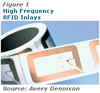
Figure 1 shows HF RFID inlays supplied in roll form. The construction of an HF RFID label comprises an HF antenna (fashioned in the form of a coil), which is then connected to the silicon chip, and the whole is supported by a film substrate. The UHF inlay design is somewhat different. Two of its components (antenna and silicon chip strap) are shown in Figure 2.
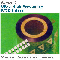
The UHF RFID antennae is supplied in roll form, as are the smaller RFID straps with silicon chips attached. The two sub-assemblies then must be connected together to create complete UHF RFID inlays.
The individual straps typically measure about 9 x 3 mm. The material is 75-micron-thick polyester (PET). Antenna footprints are significantly larger, commonly around 90 x 25 mm for an UHF design, compared to 30 x 30 mm, for example, for an HF design.
Alternatively, RFID antennae may be printed with conductive inks. This leads to a cost advantage of 30%–50% over traditional (etched or stamped) copper or aluminum antennae of comparable dimensions, while delivering equivalent performance.
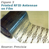
Figure 3 shows printed antennae supplied in roll form on a film substrate. RFID inlays and/or printed antennae typically are available for purchase either as an inlay for subsequent insertion by the label converter or as a completed RFID label.
Carrier Substrate Materials
A variety of film materials can be suitable for the manufacture of RFID inlay substrates, including PET, polyamide, polyvinyl chloride, or polycarbonate. Quality, performance, and reliability are critical factors for RFID inlays.
Even a very small percentage of non-performing RFID tags in a batch can be unacceptable for many applications. Specialty-grade, higher-margin materials, therefore, need to be specified. A means to prevent buildup of static electricity is a consideration.
Durability is also a consideration. The inlay substrate must support the inlay electronics as it is wound onto rolls at manufacture, unwound by the label converter, dispensed, and inserted between the layers of the label stock material. The inlay substrate must perform through all stages.
Cost Aspects
Today, the going rate for an RFID inlay embedded in self-adhesive label material typically is less than ten cents. The cost of such a finished label may be 12-20 cents for a die-cut, unprinted VIP label or up to 20-30 cents for a highly decorated prime label.
On the other hand, printed bar codes typically have a far lower incremental cost than RFID inlays, between 0.1 and 0.2 cent (estimate). Bar codes are readily printed onto labels or packaging directly, usually in the same pass as other human-readable printed data.
The aim is to achieve significantly lower cost RFID labels at five cents. This is forecast to be a commercial reality by 2010 or perhaps sooner. Further down the road, the market is looking to pay as little as one cent per unit. This will require different technology, and development is well underway. The main thrusts of such developments are aimed at eliminating the silicon chip to achieve so-called chipless RFID labels.
The 0.1-1.0 cent RFID tag will be required in order to roll out RFID label technology to lower-value, mass-retail-market, fast-moving consumer goods at individual item level. This is still a number of years in the future.
The downward evolution of unit cost of RFID labels will be driven by a succession of technologies:
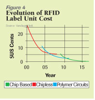
- Chip-based with traditional etched antenna/chip-based with printed antenna.
- Chipless.
- Plastic polymer electronic circuits.
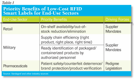
Priority benefits sought from low-cost RFID labels by end-user sectors tend to vary between market sectors as summarized in Table I. An appreciation of these issues can be helpful for new entrants to the RFID label business.
Low-Cost RFID Smart Labels—Market & Opportunities
The Vandagraf report on RFID labels contains in-depth analyses of the design, construction, and cost aspects of RFID inlays. The report also covers key drivers, such as developments in global standards and end-user mandates by Wal-Mart and the US Dept. of Defense, and key barriers, such as consumer privacy issues, radio frequency and power regulations, and data sharing across supply chains. Conclusions and quantitative forecasts are derived, supported with numerous case studies, with breakdowns by level of label application and by end-user sectors. For more information on the study, published January 2007, visit vandagraf.com.
James M. Bevan is the founder and managing director of Vandagraf Intl. Ltd., Mid-Glamorgan, UK, an international network of specialized consultants. Bevan has nearly 25 years of experience in the packaging and label sectors. Contact him at info@vandagraf.com; vandagraf.com.