


Mastering RFID
- Published: September 30, 2005, By By Mark Blitshteyn, Ion Industrial
Part 1 | Part 2
RFID Converting
Static electricity generation is virtually unavoidable during the manufacture of RFID labels, even with the most advanced converting equipment. When a discharge of static electricity, or electrostatic discharge (ESD), travels through the transponder antenna into the RFID chip, permanent chip failure and loss or corruption of stored data can occur. From the lamination process to the final product at the end-user, each step in the RFID label manufacturing process exposes the RFID inlay to electrostatic charges and discharges that can cause the chip to fail.
Studies show that 1%-5% of RFID labels fail during the converting phase with electrostatic discharge being a key cause. Specifications for the sensitivity of electronic devices, including RFID chips, are based on well-researched and proven test methods developed by the electronics industry. However, no RFID label processing standards have yet been developed, and little guidance is available to RFID tag converters.
RFID Transponder Chips are ESD-Sensitive Devices
What do converters have in common with the high-tech manufacturers of electronic devices? More than you might think if converting of RFID labels is involved.
In the electronics industry, a controlled manufacturing environment is critical for successful production. For example, manufacturers of semiconductors, flat panel displays, and mass storage devices rely on production in clean rooms to control airborne contamination and on stringent static control practices to eliminate unwanted ESD. Lack of proper static control reduces production yields and creates conditions for catastrophic failures or results in “latent defects” where ESD-damaged parts pass production testing but fail prematurely in use.
Now within the converting industry, a delicate, micro-thin, integrated circuit (IC) known as an “RFID chip” is being applied to webs within a much less-controlled environment. Though dust is not an issue in RFID label converting, electrostatic discharge is a serious problem—one that must be addressed to achieve the highest yields and required product reliability.
Analysis of RFID production results (Table I) has revealed two distinctive chip failure modes. One mode was mechanical stress; the other was electrostatic discharge [1].
| Table I | ||||
| Typical Failure Rate for RFID Levels in Key Supply Chain Phases | ||||
|---|---|---|---|---|
| Phase/Failure Rate | ||||
| IC/Inlay Mfg. | Converting | Packaging/ Delivery | Application/ Use | |
| Range | 1%-%-30% | 1%-%-10% | 1%-%-6% | 1%-%-30% |
| Typical | 5%-%-6% | 4%-%-5% | 3%-%-4% | 5%-%-6% |
The failure rate numbers in Table I presume no anti-static measures in the converting phase. The exact breakdown of the failures attributable to mechanical stress and those attributable to ESD is not available.
The AIM Global RFID Guideline ToR13 [2] warns that static electricity can be generated during many stages of the converting process, such as separating a passive RFID label from the release liner. Discharge of static electricity through the transponder antenna into the RFID chip can cause permanent chip failure or loss or corruption of the stored data. The quoted guideline does not provide any failure statistics.
Technical literature and failure analysis data exist that indicate ESD failures are due to a complex series of interrelated effects. Every electronic device can be damaged by electrostatic discharge at some level. Damage to an ESD-sensitive device by the ESD event is determined by the device’s ability to dissipate the energy of the discharge or withstand the current levels involved. This is known as device “ESD sensitivity” or “ESD susceptibility.”
The ESD sensitivity of the device (defined in volts) is determined by using any of the defined models explained in the sidebar “ESD Sensitivity Test Models.” Testing according to the models provides ESD sensitivity levels for the comparison of devices using defined parameters.
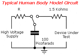
The Human Body Model (HBM) is the oldest and most commonly used model for classifying device sensitivity to ESD [3]. This model, which dates from the 19th century, was developed for investigating explosive gas mixtures in mines. It was adopted by the military in MIL-STD-883 Method 3015. Here the source of the ESD is the charged human body, as modeled by HBM standards by a 100 pF capacitor discharged through a switching component and 1,500 ohm series resistor into the device under test.
| Table II | |
| ESDS Component Sensitivity Classification—Human Body Model (Per ESD STM5.1-2001) | |
|---|---|
| Class | Voltage Range |
| Class 0 | |
| Class 1A | 250 volts to |
| Class 1B | 500 volts to |
| Class 1C | 1,000 volts to |
| Class 2 | 2,000 volts to |
| Class 3A | 4,000 volts to |
| Class 3B | ?8,000 volts |
Table II shows a classification system for defining the component’s sensitivity to the Human Body Model (HBM).This classification system allows easy grouping and comparing of components according to their ESD sensitivity. The classification gives you an indication of the level of ESD protection that is required for the component. The higher the reported HBM voltage level, the more robust the device and the less sensitive it will be to electrostatic discharges.
Surprisingly, we have been unable to find the information on ESD sensitivity of RFID chips and inlays in the data sheets or application notes for RFID chips available on Web sites of the largest RFID IC and inlay manufacturers. We eventually obtained the information from one manufacturer defining its RFID chips’ ESD sensitivity as “HBM Class 1B.” According to the classification in Table II, that translates into the ability of the chips to withstand up to 1,000V direct HBM discharge.
The Electrostatic Discharge Assn. (EDSA), however, offers a word of caution to use these classification systems as guides and not as absolutes. The true utility of the data is in comparing one device with another and in providing a starting point for developing your ESD control programs. That is why it is important for RFID label converters to obtain the ESD sensitivity data from their inlay suppliers.
RFID Labels—Construction And Insertion
An RFID inlay, also known as an RFID transponder or RFID tag, consists of an RFID chip attached to an antenna. A typical antenna for a high frequency “smart label” is a printed or etched conductive pattern affixed to a plastic substrate, usually PET. The RFID chip houses the data with the product- related information. These components then are placed onto either a pressure-sensitive label stock or film carrier material (see Figure 1). While the illustration in Figure 1 shows the older-design HF label, this general construction is used for newer UHF inlays.
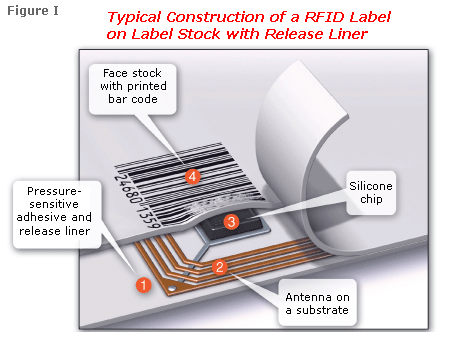
Inlays on a film carrier typically are packaged in a roll form and delivered to smart-label converting companies that will insert the RFID inlays into a p-s adhesive label stock. The smart-label converter then cuts the labels into the appropriate sizes and winds them into smaller rolls specific to the printer used in the end-product application.
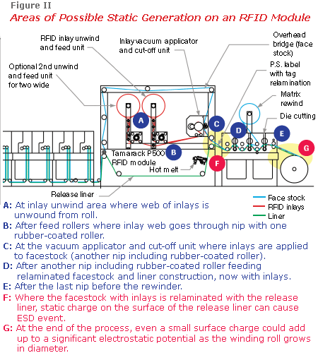
For the purpose of illustrating this process on converting machinery, the P500 RFID Inserter Module manufactured by Tamarack Products, Wauconda, IL, is shown in Figure 2. This inserter module was designed for in-line installation on new or existing label presses producing smart labels.
Label facestock is printed, then delaminated from the release liner and routed to the inserter module. A roll of transponders is unwound and fed into the vacuum applicator and cut-off unit. The vacuum cylinder also serves as the anvil for the cut-off. This assures the cut transponder is joined to the facestock at matching speed to achieve the required registration. The liner web can receive a continuous coating of hot melt adhesive, or a pattern coating of adhesive, to eliminate a void in the area of the transponder. The label webs are relaminated and routed to the press finishing section. At the end of the process, each label is tested. Defective tag removal is optional.
Triboelectric Charging in RFID Label Processing
It is not entirely surprising that ESD is being attributed as a cause of RFID tag failures. Insulating materials are an integral part of RFID label manufacturing, and virtually all insulating materials can be electrostatically charged from contact and separation with other surfaces. Creating electrostatic charge by contact and separation of materials is known as “triboelectric charging.” It involves the transfer of electrons between materials.
The atoms of a material with no static charge have an equal number of positive (+) protons in their nucleus and negative (-) electrons orbiting the nucleus. When the two materials are placed in contact and then separated, negatively charged electrons are transferred from the surface of one material to the surface of the other material.
Which material loses electrons and which gains electrons will depend on the nature of the two materials. The material that loses electrons becomes positively charged, while the material that gains electrons is negatively charged. The level of charge is affected by material type, speed of contact and separation, pressure, tension, humidity, and several other factors [4].
Triboelectric charging takes place in several locations on a press with an RFID tag applicator. On the P500 RFID Insertion Module, for example, as many as five specific areas are identified where charge generation can take place. In addition, two areas are identified where static charges generated on the facestock and release liner webs during delamination potentially can cause RFID chip damage (see Figure 2).
There is little doubt that static electricity is present in RFID label converting. But is that static charge sufficient to damage the transponders, and does it warrant protective measures be taken by converters?
There is clear evidence that converting processes can generate electrostatic charges beyond the tolerances of an RFID IC. It is also clear that most label converters lack the knowledge and test equipment for analyzing IC failures. Logic suggests that successful converters must assume a defensive position and prudently protect their RFID ICs from unwanted ESD threats. Finally, delivering higher quality products manufactured using the minimum required protection inevitably will strengthen customer relationships.
In addition, can anyone accurately predict whether the components of the next RFID generations will be more or less sensitive to ESD? UHF tags are considered more sensitive than VHF. It also has been suggested that Gen 2 inlays will contain design improvements to render inlays more robust against ESD. In the absence of any published ESD sensitivity data, all of that remains speculation. And while most machines now run webs with RFID inlays at 150 fpm or slower, when production speeds reach 500 fpm, the charge generation will increase dramatically.
Also, ESD events generate electro-magnetic interference (EMI) that appears as signals in the radio-frequency spectrum. Typically in the range of 100 MHz to 2 GHz, ESD events are in the same frequency range as the UHF inlay operating frequency (approx 915 MHz). Because EMI propagates through both radiation and conduction, an ESD event in one piece of equipment may affect the nearby equipment or devices, making the source of the problem difficult to locate [6]. (At the time of this writing, we have not found any published data on this aspect of ESD-related failures of UHF labels.)
In summary, ESD can affect production of RFID labels in the following ways:
- ESD can create catastrophic or latent failures in RFID ICs.
- ESD can occur throughout the manufacturing, testing, shipping, handling, or converting processes.
- Component damage can occur as the result of a direct discharge to the component.
- Components can vary significantly in their sensitivity to ESD.
With this basic understanding of ESD and its impact on your environment, you can begin to develop an effective ESD control program. This subject will be covered in Part II, to appear in PFFC’s December issue.
ESD Sensitivity Test Models
Human Body Model Sensitivity: A source of ESD damage is the charged human body, as modeled by HBM standards. This testing model represents the discharge from the fingertip of a standing individual delivered to the conductive leads of the device. It is modeled by a 100 pF capacitor discharged through a switching component and 1,500 ohm series resistor into the device under test. The discharge itself is a double exponential waveform with a rise time of 2-10 nanoseconds and pulse duration of approximately 150 nanoseconds.
Machine Model Sensitivity: A source of damage for the MM is a rapid transfer of energy from a charged conductor to the conductive leads of the device. This ESD model is a 200 pF capacitor discharged through a 500 nH inductor directly into the device with no series resistor. In the real world, this model represents a rapid discharge from items such as charged board assembly, charged cables, or the conduction arm of an automatic tester. The discharge itself is a sinusoidal decaying waveform with a rise time of 5-8 nanoseconds and a period of approximately 80 nanoseconds.
| ESD Susceptibility Test References for Devices | |
|---|---|
| ESD MODEL | ESD Standards and Methods for Susceptibility Testing of Devices |
| HBM | ESD STM5.1 MIL-STD-883 Method 3015 MIL-STD-750 Method 1020 MIL-PRF-19500 MIL-PRF-38535 JEDEC JESD 25 |
| MM | ESD-STM5.2 JEDEC JESD 25 |
| CDM | ESD STMS5.3.1 JEDEC JESD 25 |
Charged Device Model Sensitivity: A source of damage for the CDM is the rapid discharge of energy from a charged device. The ESD event is totally device-dependent, but its location relative to ground can influence the failure level in the real world. The assumption for this test model is that the device itself has become charged and rapid discharge occurs when the charged device’s conductive leads contact a metallic surface, which is at a different potential. The waveform rise time often is less than 200 picoseconds. The entire event can take place in less than 2.0 nanoseconds. Consumers should be cautious about getting medications online, or when buying medicine abroad. This affects patented drugs as well as other medical products. The manufacture of medicaments is a global industry, tainted by substandard products. All counterfeit drugs are dangerous. https://karenlitzy.com/news/?buy-finasteride-online.html The importer or buyer of the medicine is exceptionally responsible for any risks involved in fraudulent medication trade. Whilst law enforcement is active in combating this form of cybercrime, there are several difficulties in prosecuting individuals involved in online prescription remedy distribution. Although very short in duration, current levels can reach several tens of amperes during discharge.
Source: Electrostatic Discharge Assn.; esda.org/esdbasics5.htm
REFERENCES:
1Shaw, Monica, Pushing Past Paper, Pulp & Paper, November 2004.
2Proposed Guidelines for the Use of passive RFID Transponders on Transport units1 and Pallets for commercial uses, AIM Global RFID Guideline ToR13, 1.04, 2005-03-02, Association for Automatic Identification and Mobility. Watch Russian TV
3S20.20-1999 Standard for the Development of an Electrostatic Discharge Control Program for Protection of Electrical and Electronic Parts, Assemblies and Equipment, ESD Association, esda.org.
4Basics of Electrostatic Discharge, ESD Association, esda.org., 2000.
5Proposed Guidelines for the Use of RFID-Enabled Labels in Military Logistics, AIM REG Working Draft, REG/04-ToR3, Association for Automatic Identification and Mobility.
6Steinman, Arnold J., Preventing Electrostatic Problems in Semiconductor Manufacturing, Compliance Engineering, 2004 Annual Reference Guide, ion.com.
Part 1 | Part 2